Level Shifter Cell:
- In most of the Low Power Designs, there are one or more power domains where we have more power domains which operates at different voltage level in a single partition. In this case, we need different voltages to operate these logic groups. The problem is that we cant afford too many power supply in the same design. So, to solve this situation we need some circuit which will help us in getting the required voltages wherever needed. This circuit is named as level shifter. From the name itself, we can deduce that the circuit shifts the level.
- Level shifter cells are present in the Netlist and are placed near to the port. These cells are mostly buffer type or latch type. Level shifter cells are defined in UPF according to requirement of different voltage domains.
- It is easy to get the high to low LS cell but low to high LS cells are complex and larger in size as compared to high to low LS cells. (It’s easy to destroy something but hard to gain)
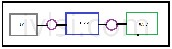
- The below picture explains about the 3 Voltage domains present in the design. The first operates at 1 V, second at 0.7 V and third at 0.9 V in the same design.