The physical design flow in VLSI is where your chip design starts coming to life. After the synthesis stage, it’s time to take your design from a logical blueprint to a physical layout that can actually be fabricated on silicon. This phase is intricate, involving specialized tools, precise inputs, and detailed steps to ensure everything works perfectly.
Let’s break down the key inputs you need to kickstart physical implementation.
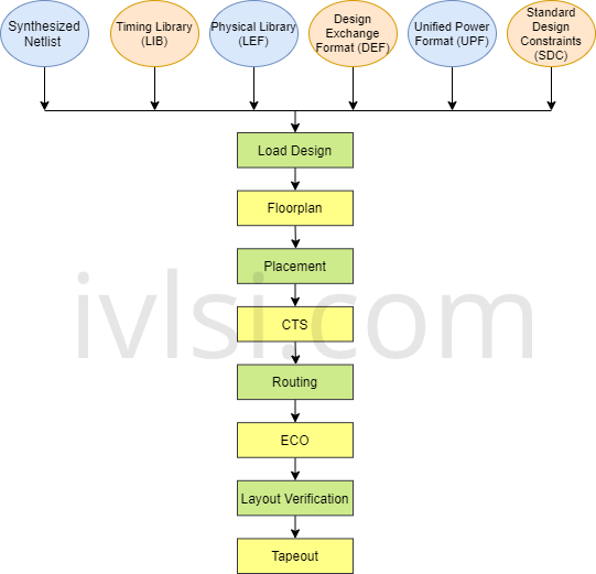
6 Must-Have Inputs for Physical Implementation
To ensure a smooth physical design process, here’s what you need:
- Synthesized Netlist:
This is the output from the synthesis stage. Think of it as the digital map of your design, showing how all the logic gates and connections fit together. It’s the starting point for your physical layout. - Timing Library (.lib):
Timing is everything in chip design! This file provides the timing details for your standard cells—like delays, setup times, and hold times—so your design can run at the desired speed. - Library Exchange Format (LEF):
The LEF file tells the tools the physical details of your cells: dimensions, pin locations, and metal layer information. Without it, your design tools wouldn’t know where or how to place each cell. - Unified Power Format (UPF):
Power management is a big deal in modern chip design. The UPF file lays out the power intent, like defining power domains, voltage levels, and how power gating is handled. - Design Exchange Format (DEF):
Think of the DEF file as a snapshot of the physical placement of your components. It ensures everything is positioned correctly, setting the stage for routing and optimization. - Standard Design Constraint (SDC):
The SDC file defines timing constraints for your design. From clock definitions to input/output delays, it helps ensure your chip hits all its performance targets.
Why These Inputs Are Game-Changers
Every one of these inputs plays a critical role in your physical design flow. They guide your tools in crucial steps like floorplanning, placement, routing, and timing closure. When done right, these inputs ensure your design meets the holy grail of chip design: performance, power, and area (PPA).
By starting with the right foundation, your physical design flow becomes smoother, faster, and more efficient—leading to a chip design that’s not just functional, but optimized for real-world success.
Ready to take your VLSI design to the next level? This is where it all starts!
The physical design flow in VLSI is where your chip transforms from an idea into a tangible, manufacturable product. Every stage in this process is critical to ensure the final chip meets performance, power, and area (PPA) requirements while remaining manufacturable. Let’s walk through the key stages of this process and the tools that make it happen.
Physical Design Flow Stages
1. Floorplanning
Floorplanning is all about defining the chip’s high-level layout. Key elements include:
- Placing pins for I/O.
- Creating power stripes and rings for power distribution.
- Positioning physical cells like macros, boundary cap cells, tap cells, and isolation cells.
A well-executed floorplan lays the foundation for the rest of the physical design process.
2. Placement
Placement involves arranging standard cells within the core boundary. This stage ensures cells are optimally positioned for:
- Performance.
- Signal integrity.
- Area efficiency.
Challenges like cell overlap, density, and timing slack are addressed here.
3. Clock Tree Synthesis (CTS)
CTS is where the ideal clock becomes a real clock network. Key considerations include:
- Minimizing latency: Ensuring quick clock signal propagation.
- Balancing skew: Equalizing clock arrival times across the design.
- Reducing power: Efficient clock routing.
- Ensuring duty cycle: Achieving proper signal ratios for reliable performance.
4. Routing
Routing connects the pins of cells using metal layers. This stage ensures:
- Accurate electrical connectivity.
- Proper signal flow across the design.
- Adherence to design rules for the specific technology node.
Routing is critical to achieving an electrically and physically viable design.
5. Sign-Off and Verification
After routing, the design undergoes rigorous sign-off processes:
- ECO (Engineering Change Orders): Fixes timing violations, electrical issues, and layout concerns.
- Physical DRC/LVS Cleanup: Ensures the design complies with layout design rules and matches the schematic.
6. Fabrication
Once the design passes all sign-off checks, including DRC/LVS and timing analysis, it’s sent for fabrication. This is the final step before your chip becomes a reality.
Tools and Techniques
Here’s a breakdown of industry-standard tools used in the physical design flow:
- Synthesis: DC (Synopsys), Genus (Cadence).
- Formal Verification: LEC (Cadence).
- Physical Design Implementation: Innovus (Cadence), ICC2 (Synopsys).
- Timing Analysis: Prime Time (Synopsys), Tempus (Cadence).
- DRC/LVS Analysis: ICV (Synopsys).
- Library Characterization: Liberty (Cadence).
Each tool is specialized for a specific stage, ensuring efficiency and precision throughout the flow.
Conclusion
The physical design flow in VLSI is a multi-stage process, where each phase builds upon the previous one to create a manufacturable and functional chip. From floorplanning to fabrication, every step plays a critical role in achieving PPA goals and ensuring design integrity.
By leveraging advanced tools and techniques, you can streamline this process and achieve optimal results. Whether you’re a beginner or an industry professional, mastering these stages is key to building high-performance VLSI chips that succeed in the real world.