Power Switch Cell Placement
- Power switch cells are physical only cells. Basically power switches are defined in UPF w.r.t power domains present in the design.
- We need power switch in the design to control the power depending upon the power domain requirement.
- Power switch avoid inrush current which helps in STD cell damage.
- As we know, there are power domains which are Always-on, these power domains do not need power switch in the design.
- Before placing the power switch in the design, we specify the Pitch, Offset and orientation to place PSW cells.
- Power switch cells are placed in the design in daisy chain scheme and their placement starts from bottom left.
- We can re-chain power switch based on requirement if the daisy chain has been broken in between due to other design issues.
- There are four pins in the power switch as per below:
- Enbl_few
- Enbl_rst
- Awk_few
- Awk_rst
- Header and footer circuit are used to create one power switch.
- Mostly industry uses header power switch because we control main supply.
- Power switching is a technique that reduces leakage power by cutting the flow of current between VDD and VSS while the circuit block is idle.
- Control over IR drop.
Drawbacks
- Consumes area.
- Increases congestion in some areas.
- Power grid complexity increases.
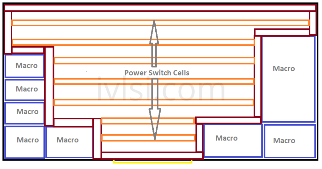
In the above figure we can see that power switch cells are placed in array pattern in rows.