- Also known as a gate-level netlist. It contains all the gate level information and the connection between these gates.
- It can be flat or hierarchical.
- Flat Netlist contains only one module with all the information.
- Hierarchical netlist contains a number of modules and these modules are being called by one module.
- Example:
The second part is to understand that, in these input/output pins what are in input categories and what are in output categories like below. Along with this, it defines the pins which helps to transfer the data like buffer named wire.
input clk, rst, SE, scan_in;
output [7:0] count;
output scan_out;
wire clk, rst, SE, scan_in;
wire [7:0] count; wire scan_out;
wire n_0, n_1, n_2, n_3, n_4, n_5, n_6, n_7;
wire n_20, n_21, n_22, n_23, n_24, n_25;
assign scan_out = count[7];
This statement says count[7] output is being assigned to scan_out.
SDFFRHQX1 count_reg[0] (.RN (rst), .CK (clk), .D (n_6), .SI (scan_in), .SE (SE), .Q (count[0]));
This statement says that D Flip-Flop SDFFRHQX1's connections. Where SDFFRHQX1 is cell name and count_reg[0] is the instance name. The cell name is what we pick from the library and can be used any number of times in designs but the instance name is always one for a particular design.
RN is connected to input pin rst which we have defined above. Similarly, CK is connected to clk , D is connected to n_6, SI is with scan_in, SE is with SE and finally, output is connected to count[0]. Similarly for other flops connection has been defined.
INVX1 g769(.A (count[0]), .Y (n_6));Similar to DFF INV and other cells are also defined in this way.
Finally, we are done with the cells and all the connections, so will go for endmodule.
Let's look at the image of the circuit w.r.t to the above counter 8-bit netlist.
[caption id="" align="alignnone" width="1149"]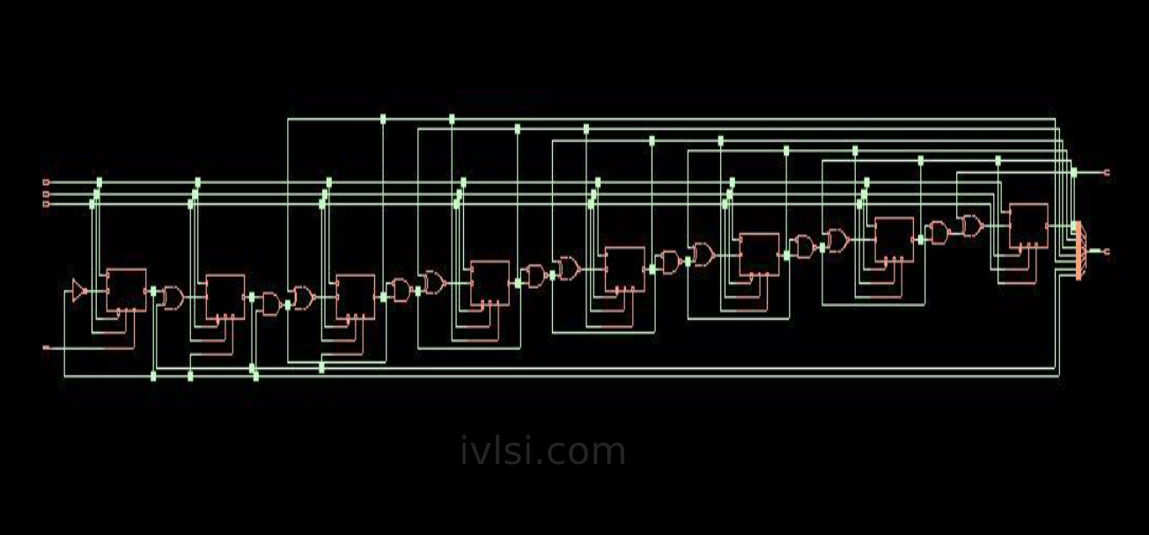 Counter 8 Bit Circuit[/caption]
Let's take one more example, this one will explain a lot about the real designs.
 module ivlsi (
        clk_proc, as_rst_n, token_i, a[27] , a[26] , a[25] , a[24] ,
        a[23] , a[22] , a[21] , a[20] , a[19] , a[18] , a[17] , a[16] ,
        q[4] , q[3] , q[2] , q[1] , q[0] , atpg_ctrl,
  DFT_IB_DFT_out_demod_reg_en_accu_d_cgc_clk_en_buf7_z_cnt7_iso_mux_sel,
        clk_en_power_gating_cnt211_b, test_si4, test_si3, test_si2, test_si1,
        chain_si18, chain_sel18, DFT_ib_top_comp_depth_mode18_bypassmux_a );
  input clk_proc, as_rst_n, token_i, a[27] , a[26] , a[25] , a[24] ,
         a[23] , a[22] , a[21] , a[20] , a[19] , a[18] , a[17] ,
          DFT_IB_DFT_out_interniso_u_demod_reg_en_accu_d_cgc_clk_en_buf7_z_cnt7_iso_mux_sel,
         clk_en_power_gating_cnt211_b, test_si4, test_si3, test_si2, test_si1,
         test_se, ctcm_scan_en_ib, chain_si18, chain_sel18;
  output token_o, q[27] , q[26] , q[25] , q[24] , q[23] , q[22] ,
         q[21] , q[20] , q[19] , q[18] , q[17] , q[16] , q[15] ,
          test_so3, test_so2, test_so1,
         DFT_ib_top_comp_depth_mode18_bypassmux_a;
  wire   N1, net834978, n10, n4, n6, n8, n9, n7, n3;
ivlsi_cell1 aq_reg[28]  ( .d(token_i), .sin(n7),
        .shift(ctcm_scan_en_ib), .clk(net834978), .rst(n3), .q(token_o) );
  ivlsi_cell2 aq_reg_FTREG8_30342 ( .clk(net834978),
        .d0(a[0] ), .d1(a[1] ), .d2(a[2] ), .d3(a[3] ), .d4(a[4] ),
        .d5(a[5] ), .d6(a[6] ), .d7(a[7] ), .rst(n3),
        .shift(ctcm_scan_en_ib), .sin(test_si2), .q0(q[0] ), .q1(q[1] ),
        .q2(q[2] ), .q3(q[3] ), .q4(q[4] ), .q5(q[5] ), .q6(q[6] ),
        .q7(q[7] ), .sout(n9) );
  ivlsi_cell3 aq_reg_FTREG8_30343 ( .clk(net834978),
        .d0(a[8] ), .d1(a[9] ), .d2(a[10] ), .d3(a[11] ), .d4(a[12] ),
        .d5(a[13] ), .d6(a[14] ), .d7(a[15] ), .rst(n3),
        .shift(ctcm_scan_en_ib), .sin(n9), .q0(q[8] ), .q1(q[9] ),
        .q2(q[10] ), .q3(q[11] ), .q4(q[12] ), .q5(q[13] ), .q6(q[14] ),
        .q7(q[15] ), .sout(n8) );
endmodule