CTS Spec File
CTS spec file contains the below information:
1. Inverters or buffers to be defined which will be used to balance the clock tree.
2. CTS Exceptions (End points of clock tree).
3. Skew group information.
4. Contains target Skew, max target transition and other timing constraints as per clock tree.
5. Top layer and bottom layer route info. VIA's information which will be used during clock route.
6 Clock related info (Generated clocks {Eg. Clock divider, Clock multiplier etc}).
7 NDR Rule definition.
1. Inverters or buffers to be defined which will be used to balance clock tree:
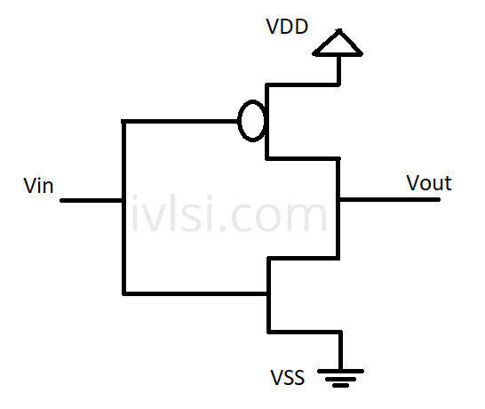
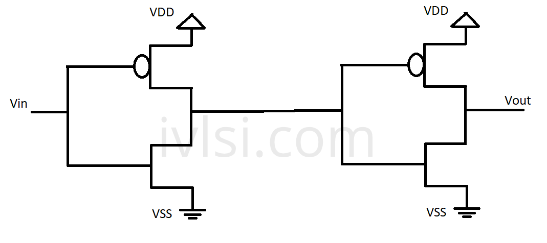
When I was in the early stage of VLSI industry, I always thought that buffer is the only element which is used for the clock balancing but when I worked on designs, I saw that Inverter plays a very important role in balancing. So, we can say that while balancing the clock tree, we can use both buffer and inverter. Normally inverter is used more in the design. Before understanding why inverter is better than buffer, first we need to recall the difference between a buffer and an inverter. (This might be an interview question and I have asked this to many candidates)
Buffer is basically two inverters connected back to back. So, wherever we need to use one buffer, we can split that buffer into two inverter which balances better in terms of transition and consumes less power and area. For example, if we need 30 buffers to balance a tree and these are back to back connected, then in this case, we can use 60 inverters instead of 30 buffers. But practically we don’t need 60 cells, so our requirement can be met within 30-40 inverters. This way we can save power and area along with making transition better for clock.
2. CTS Exceptions (End points of clock tree):
There are many points present in the design after which we don’t need clock tree propagation. So to avoid unnecessary buffering, we can ask the tool not to go for balancing further to these points.
3. Skew group information:
There are millions of sink pins which we need to balance in the design. There might be a case where design is huge, and we will have high latency. So to avoid this, we create skew group. We will talk more details on creating and executing skew group later in this section.
4. Contains target Skew, max target transition and other timing constraints as per clock tree.
Spec file contains the skew values defined, max and min transition of the clocks along with other timing constraint.
5. Top layer and bottom layer route info. VIA’s info which will be used during clock route.
While creating clock tree, we need to route the clock. So we need to define the routing layers. Generally we choose top metal layers for clock routing as these metal layers have lower resistance as compared to lower metal layers.
6. Clock related information (Generated clocks {Eg. Clock divider, Clock multiplier etc.})
If we have missed defining generated clock in the SDC, we can define it here while balancing the clock.
7. NDR Rule definition:
Clock nets are very sensitive and impacts timing if it changes a little. We already have default rule present in the design but if we route with default rule, we might have many issues like crosstalk, transition violations, min pulse width issues at the end. To avoid all these issues in later ECO stages, we define the NDR rule. Non-Default Rule (NDR) means that other than default rule, it contains some user defined routing rule like Double-Width Double Spacing, single width double spacing etc.