What is a Clock?
A clock signal is like the heartbeat of a digital system. It pulses at regular intervals, switching between high and low states with steady rise and fall transitions. In an ideal case, the clock has a 50% duty cycle, meaning the time spent high and low is equal. This rhythm is what keeps the system in sync, guiding data as it moves through clocked elements like flip-flops and latches, and ensuring everything happens at the right moment.
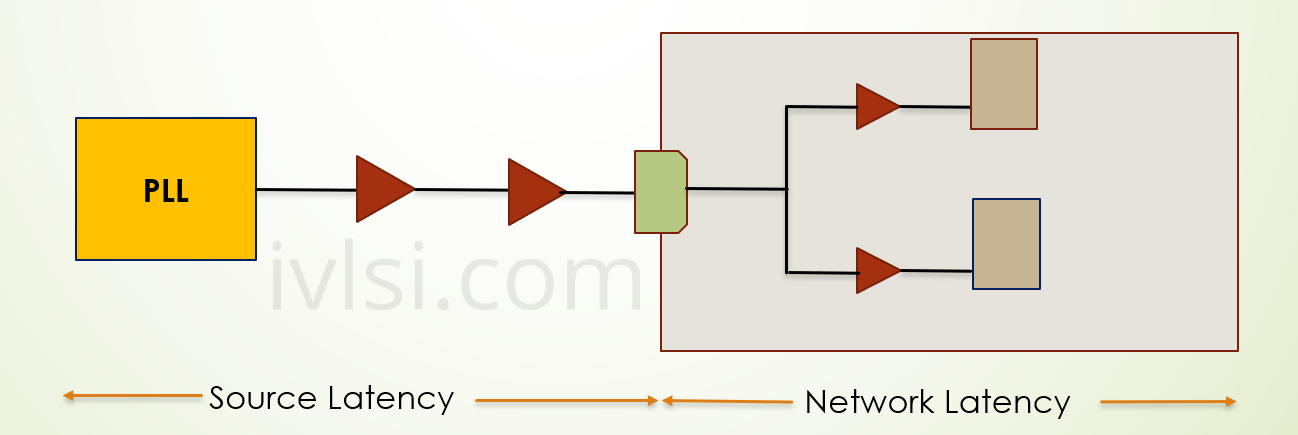
Clock sources are usually placed at the top level of a design and propagate through the circuit using PLL (Phase Locked Loop), Oscillators, or other constant sources.
Since clock signals directly impact timing and performance, careful handling is required. In the SDC (Synopsys Design Constraints) section of physical design, we define the clock. However, defining a clock isn’t enough—clock propagation must be balanced to ensure all clock elements switch at the same time. This is where Clock Tree Synthesis (CTS) comes into play.
Why Do We Need Clock Tree Synthesis?
Before CTS, the clock path behaves ideally, meaning there is an equal delay from the clock source to all endpoints. But in reality, variations in wire lengths and routing cause clock skew, which can impact performance and reliability.
CTS automates the insertion of buffers/inverters along the clock path to balance delays and ensure even clock distribution across sequential elements.
Inputs for Clock Tree Synthesis
CTS requires two major inputs:
- Placement Database (DB):
- Contains Netlist, DEF, LIB, LEF, SDC, UPF, and other placement-related information.
- This is also called PLACE EXIT DB, meaning no further standard cell placement occurs after this stage.
- CTS Specification File:
- Defines inverters/buffers for clock balancing.
- Lists CTS exceptions (e.g., endpoints of the clock tree).
- Contains skew group information.
- Sets target skew, max transition, and other timing constraints.
- Specifies routing layers, VIAs, and NDR (Non-Default Rules).
- Defines clock modifications (e.g., dividers, multipliers).
How Clock Tree Synthesis Works
CTS follows multiple strategies to ensure balanced clock propagation. The most widely used Clock Tree Algorithms include:
- Fishbone Tree
- H-Tree (Most common, explained below)
- Clock Mesh
- Spine Tree
H-Tree Algorithm Steps
- Identify all flip-flops in the design.
- Find the geometric center of all flip-flops.
- Trace the clock port to the center.
- Divide the core area into two halves and trace each part to its center.
- Continue dividing until you reach each flip-flop's clock pin.
- Insert buffers/inverters at each division point to balance delays.
Advantages of Standard H-Tree
- Good cross-corner scaling behavior
- Well-balanced by construction
- Lower power consumption than mesh-based CTS
Disadvantages of Standard H-Tree
- Requires a power-of-two number of sinks (buffers)
- Needs a rectangular unblocked area
- Higher power than an ad-hoc CTS tree
Flexible H-tree – Limitations:
You will need to determine where to insert H-tree(s) in the clock architecture
- Requires clock architecture understanding
- User specified root pin
- User specified pre-existing leaf pins or sink grid area for new leaf buffers
- Newly inserted leaf buffers become tap buffers for multi-tap CTS
- The flexible H-tree only contains buffers or inverters
- No logic or gating
Before going for the clock tree design, we need to have sanity checks where we look for following:
- Design is placed or not. Place Exit should complete.
- Clocks has been defined.
- Clock roots should not be on hierarchical pins.
Clock Tree Synthesis Steps
There are following steps which need to be performed during the Clock Tree Synthesis:
- Clustering
- DRV Fixing
- Insertion Delay Reduction
- Power Reduction
- Balancing
- Post-Conditioning
Clustering
Depending on the geometry locations, the skew groups are being created as per the description in SPEC file.
DRV Fixing
At this stage, DRVs (max_tran, max_cap, max_length, max_fanout) are fixed.
Insertion Delay Reduction
At this stage, insertion delay is getting minimized as much as possible, which is one of our main goals for the Clock Tree Synthesis.
Power Reduction
As we know clock is a major power consumer, so we need to analyze and fix it in such a way that power consumption will be less.
Balancing
The main balancing happens at this stage with the help of different clock buffers and inverters.
Post-conditioning
At this stage, again DRVs will be checked and if required then it will be fixed.
CTS Quality Checks
There are following quality checks for the Clock Tree Synthesis:
- Minimize Insertion Delay
- Skew Balancing
- Duty Cycle
- Pulse Width
- Clock Tree power consumption
- Signal Integrity and Crosstalk
Let’s discuss these topics in details:
Minimize Insertion Delay
Advantages of the low Latency:
- Less buffer, hence less power consumption. As we know clock paths are the heaviest power dissipated path.
- Cell area reduction as less buffer in the clock path.
- Less runtime since less buffer need to be inserted in the design, which saves optimization as well.
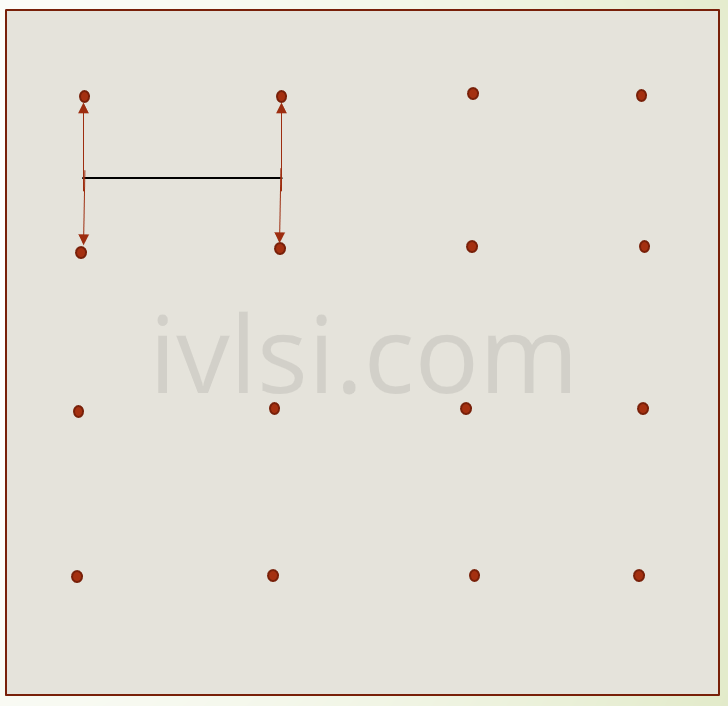
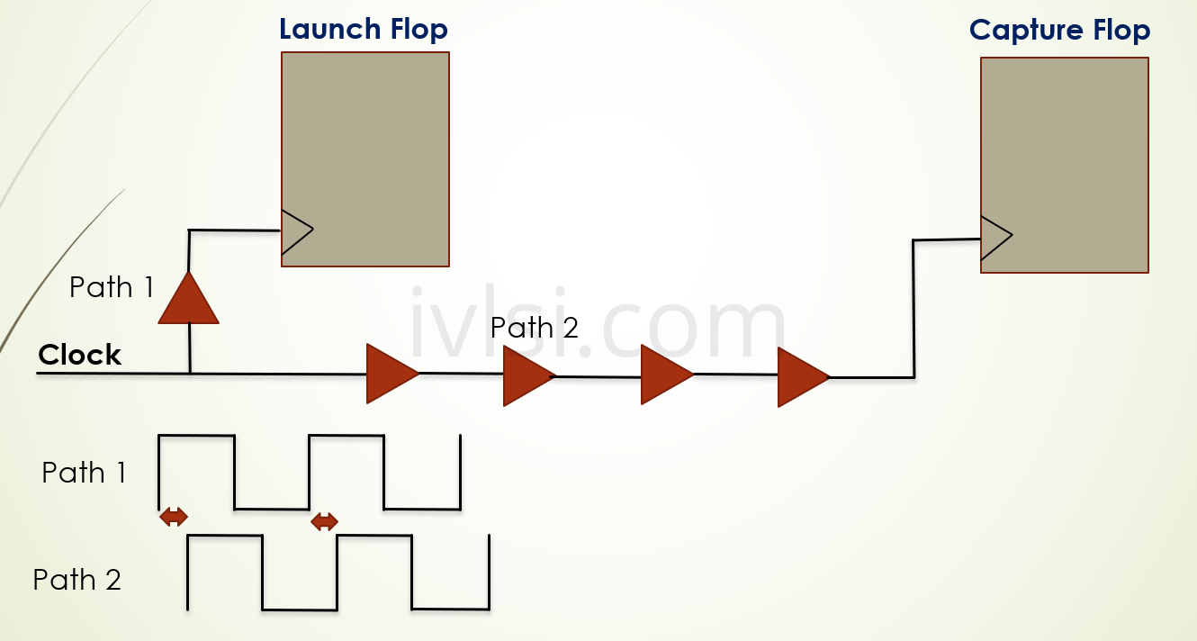
Skew Balancing
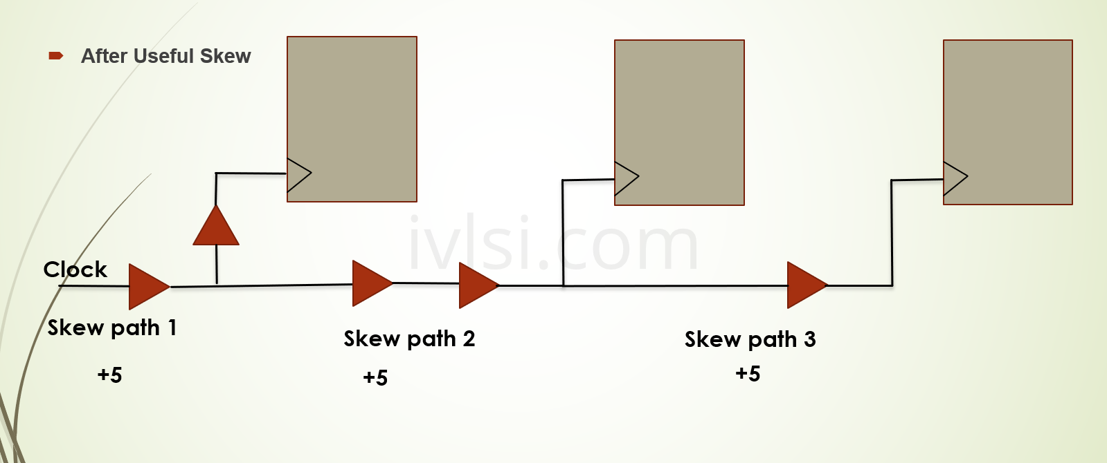
Skew: Skew is the difference of time between the clock path. Let’s understand more through the picture.
Useful Skew
Useful skew is very important concept in CTS. Let's discuss this through an example.
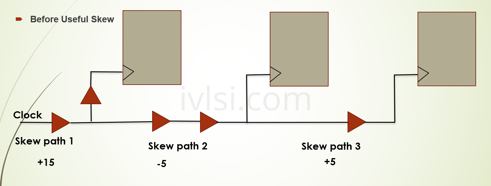
In the above picture, we can see that the first path is having positive 15 ps of skew, second path is having negative 5 ps of skew and third is having positive 5 ps skew. Now, if we can see among these three paths, the negative path can borrow skew from the first positive 15ps path, then skew will be balanced between the paths. After borrowing the skew, we can see that in below picture the skew looks positive in number for all the three paths. This concept is called as useful skewing and the skew we borrowed is useful skew.
Duty Cycle & Pulse Width
https://ivlsi.com/duty-cycle-pulse-width-vlsi-physical-design
Clock Tree Power Consumption
As we know that clock network is the heaviest switching element in the design.
Clock tree power depends upon below two factors:
o Latency
o Transition
Signal Integrity & Crosstalk
https://ivlsi.com/signal-integrity-and-crosstalk-vlsi-physical-design
1. Latency: If latency is less then less buffer in the design. So less power consumption.
2. Transition: If transition is good then less power consumption. Transition is being blamed always for the losses happening in the design w.r.t the trade-off.
Runtime:
- Runtime depends upon how much time it takes to build the clock tree in a design. Optimization w.r.t to the QOR results and routing of the clock nets.
- Basically, during optimization, we loss more time if we are having more tight constraints and we need to spend more time to achieve the targets after clock tree building. As we have setup and hold, both need to be taken care of, so timing optimization takes more time.
Clock Tree Structure
The clock tree has been divided into three parts- Top, Trunk, Leaf to understand deeper into the CTS quality and balancing. Below is the picture explaining the clock tree structure.
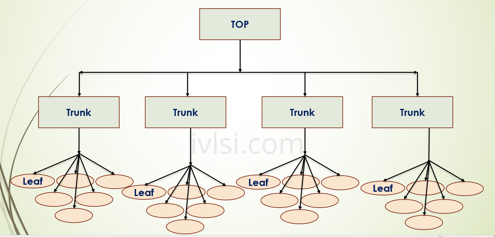
Clock Tree Network
Clock tree information can be as per below:
- A transitive fanout of a root pin.
- A sink can belong to more than one clock tree.
Root pins: The starting point of the clock signal.
Internal Pins: The pin with which clock propagation happens from root to sink.
Sink Pins: The terminal point of a clock signal. Or sequential element pins or stop pins or Ignore pins.
Clock Tree Exceptions
There are following clock tree exceptions:
Stop Pin – No buffer/inverter insertion beyond this point (Don’t touch scenario)
Ignore Pin (Float Pins) – No DRV, No Balance
Exclude Pin – DRV Fixing but no balancing
Through Pin – DRV Fixing as well as Balancing
Timing Analysis and fixing
As we know the best approach is to look at the problem and analyze the root cause before going to solve it. So first see few sets of issues which can cause the timing violations after Clock tree synthesis.
Below can be the reason for a broken timing, let’s investigate it in details:
Clock Latencies, skews and uncertainties
- What is uncertainty vs. clock period?
- Are the different clocks correctly balanced (unless there are false paths)?
Cell distribution over the path
- Are there suspiciously long buffering chains (>10 buffers back to back)?
- Is it a short (< 5 instances) or a deep logic level path (> 30 instances)?
- Are the drive strengths chosen correctly?
- Are the correct library cells being used (fast cells for timing critical paths)?
Net load, slew, fanout and wire length
Instance and net delay
- Are there instances or nets with unexpected large delay (> 5x) compared to others?
Net and Cell derating
- Are the derating values realistic? (between 0.8 and 1.2)
Congested region
- Do we have congested region in a particular area from where clock buffer/inverter was not able to place there and went far away? If yes, then we need to de-congest that area so that clock buffer/inverter should get proper physical location to get placed. Placement or routing congestion both can make the timing broken.
- Is the placement compact or widely spread over the floorplan?
- Are the instances correctly spread from the start point to the endpoint?
- We need to look at the path topology whether it is straight or detoured.
- The channels we created during floorplan are sized correctly or not.
- Does the path cross the power domains or getting detoured due to huge Marcos present in the design?
- Many times, power domain shapes matter. So it's good to check the shape of power domain and ensure that it’s not too big or too small. I personally have faced this issue many times. So we need to take care of power domain shape in order to converge timing.
As we have looked into many reasons, let's see what are the steps we can use to debug timing in the design at post-CTS stage:
- Look into timing debug window of any tool for the worst negative slack path.
- Check the path and understand the driver and receiver cell and the cells present in the path.
- Look for the insertion delay and check if some cells having high delay value.
- Check the location of that particular cell in the design. Are they too far from the driver? Is the net having detour?
- Has the leaf (Driver) cell got stuck into some channel of macros or near high placement congested area?
- Check the issue why this cell has got high insertion delay and got detoured. If possible, block the area with hard blockage if it is a channel in between the macros.
Integrated Clock Gating (ICG) Cell and related concepts
https://ivlsi.com/integrated-clock-gating-icg-cell-and-related-concepts-vlsi-physical-design
Clock Tree Route and NDR
Once we are done with the clock tree balancing after all the clock cells placement, we go for the final routing of the clock nets and fix it. After clock routing, whatever is left out will be used for signal routing. Now the question is which metal layers to be used and how we should do routing to avoid issues in later stages.
Generally, we use mid layers like M5 - M8 of TSMC 7nm where M0-M13 metal layers are available for clock routing. We know that higher metal layers have low resistance as compared to the lower metal layers but still why did we stop at M5-M8?
Normally we use M12, M11, M10, M9 for power routing and then remaining for clock routing. Also, using a stack of vias is also another issue hence M5-M8 is the best choice for clock routing.
There is always a defined metal width and spacing from foundry which is being used for routing, but if required we change the width and spacing for the metal layers to achieve our PPA target. We can increase the width and height but can’t use lower than what foundry has proposed.
During clock building, our target is timing and Power as well, since clock is continuous signal, it consumes more power. So in order to achieve good PPA, we require non-default-routing rule. Normally we use double width and double spacing for clock routing, however this might change depending on the requirement.
Final Thoughts
Clock Tree Synthesis (CTS) is a critical stage in physical design, ensuring balanced clock distribution, minimizing skew, and optimizing power consumption.
By following best practices and fine-tuning clock routing, designers can achieve efficient, high-performance digital designs while reducing power and avoiding costly timing violations. 🚀