During placement, following three stages happens:
- Global Placement
- Refine Placement (Legalization)
- Detailed Placement
Global Placement
Global placement is very first stage of the placement where cells are placed inside the core area for the first time looking at the timing and congestion. Global Placement aims at generating a rough placement solution that may violate some placement constraints while maintaining a global view of the whole Netlist. There may be overlap among the modules.
- Core Placement + Timing Analysis + Congestion Analysis
- There are following points that need to be taken care during the global placement:
1. Fix High Fanout
2. Logic Restructuring
3. Scan re-ordering
4. Fix Input Transition
Fix High Fanout
- Number of gates connected from an output of a driver cell is known as Fanout. Fanout is basically a number of gate input which the output is safely connected.
- High fanout load means there are more number of loads which is being driven by a single output of a gate. Loads more than desired leads to number of issues in the design.
- SDC command “set_max_fanout” helps to constrain the output to set it to some max limit of fanout.
- We can optimize the fanout on violating nets by either upsizing driver instance or by splitting load by adding a similar instance at this stage. We will discuss this more into ECO phase.
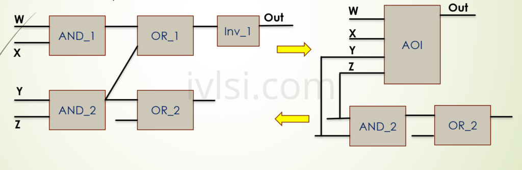
Logic Restructuring
- Placement engine restructure the netlist if there are timing benefit. The optimization engine evaluates the impact of restructuring on congestion, power, area etc. Restructuring means Gate composition or decomposition.
- E.g. – Gate Composition – AND/OR/INV => AOI
Gate Decomposition – AOI =>AND/OR/INV
Scan Re-ordering:
Before going to understand the scan reordering, lets understand first what is scan chain and how it works.
Scan Chain:
- The purpose of adding scan chains is to make the flip-flops in the design controllable and
observable. - When the SEN signal in the example below is asserted (set to 1), every flip-flop in the design
becomes part of a long shift register and the expected value that is shifted out is compared to
the actual value.
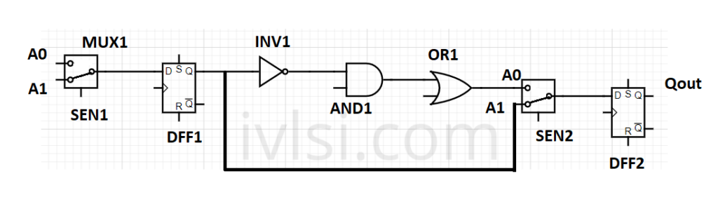
Let’s take below circuit which consists of 2 DFF, where there is small combinational circuit present in between the flops. Normally when scan chain has not been inserted, then circuit fully operates for functional.
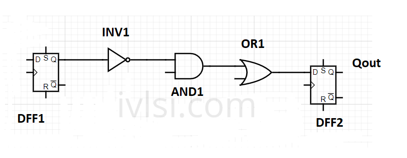
Once Scan chain will be inserted then muxes will be inferred and the select line of mux will control the functional and scan propagation. If SEN =0, then A0 will be propagating at this time & we can say this is functional propagation and if SEN=1 then A1 will be propagating, it will be scan path. In the below circuit, we can see that SEN1 and SEN2 are in 0 state and hence A0 is getting propagated, which means functional propagation happens here. Now the path is A0 -> DFF1 -> INV1 -> AND1 -> OR1 -> Mux2 -> DFF2, which says how the logic propagation happens in functional mode.
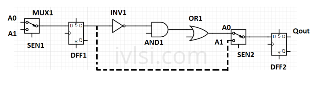
Now if SEN1 and SEN2 is 1 then A1 will be propagating and the path will be a scan path. So, the path will be as A0 -> DFF1 -> Mux2 -> DFF2.
Scan DEF Example:
NAMESCASESENSITIVE ON;
DIVIDERCHAR “/” ;
BUSBITCHARS “[]” ;
DESIGN ivlsi_test ;
SCANCHAINS 2 ;
-AtoChain_1_seg1_clk1_rising
+ START PIN DFT_sdi_1
+ FLOATING
Out1_reg_0 ( IN SI ) ( OUT Q )
……..
Out1_reg_74 ( IN SI ) ( OUT Q )
+ STOP PIN DFT_sdo_1;
-AutoChain_2_seg1_clk1_falling
+ START PIN DFT_sdi_2
+ FLOATING
Out2_reg[0] ( IN SI ) ( OUT QN )
………
Out2_reg[99] ( IN SI ) ( OUT QN )
+ STOP PIN DFT_sdo_2;
In the above DEF, we can see that there are two scan chains with START and STOP keyword that denotes the starting and the ending point of the scan chain.
Scan Re-Ordering
Now we know how scan chains are being inserted and how it effects the circuit. Now let’s focus on the main topic that is, how tool optimizes the scan chain.
Reordering of the scan chain helps optimizing the routing resources and make design decongested. Lets take one example of before and after scan chains and see how the routing resources are being saved.
Before Scan Reordering
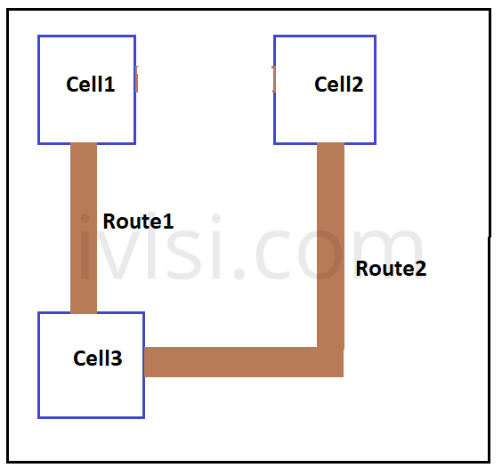
In the above figure, we can see that route 1 and route2 completes the scan chain routing which is comparatively longer route than after scan chain reordering where we have small route length completing our requirement. During placement optimization, tool does these optimizations to save route tracks for the clock/signal routing at later stages.
After the scan reordering
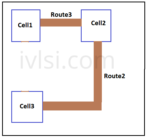
we have less routing congestion and is getting estimated by trial route run.
Fix Input Transition
- Delay depends upon input transition and output capacitance. So if high input transition is there, then we will see more delay in the design. SDC command “set_input_transition” sets the transition value, so if input pin transition go beyond the number then that creates violations.
- Transition can be fixed using below methods:
- Reduce wire length by placing cells near to each other.
- Add buffer in the transition violated path.
- Split buffer into inverters and place with some distance.
- Assign higher metal layers to all the nets to the tran violated nets. (Layer promotion)
- Upsize driver instance by increasing the drive strength.
We will discuss more in details about this in ECO phase.