Power
We will discuss more about power analysis in ECO section while working on PDN, for now let’s take basic glimpse of the power analysis and consumption.
There are basically 2 types of power consumption in VLSI design:
1. Dynamic Power Dissipation
2. Static Power Dissipation
1. Dynamic Power
There are two types of dynamic power consumption in digital circuits.
a. Switching power
Switching power basically depends upon frequency of design/net, load capacitance and Power supply (VDD).
Switching power = α * F * C * (VDD)²
In the above equation we can see that switching power depends on below factors:
α -> Alpha a factor, normally value is ½ (0.5).
F -> Frequency of the design
C -> Load capacitance
VDD -> Power
We can use the following techniques to reduce dynamic power:
- Sequential cell downsizes
- Gate composition transform
- Pin swap transform
- Avoid long routing
- Merge cells in terms of nets
- Use higher metal layers
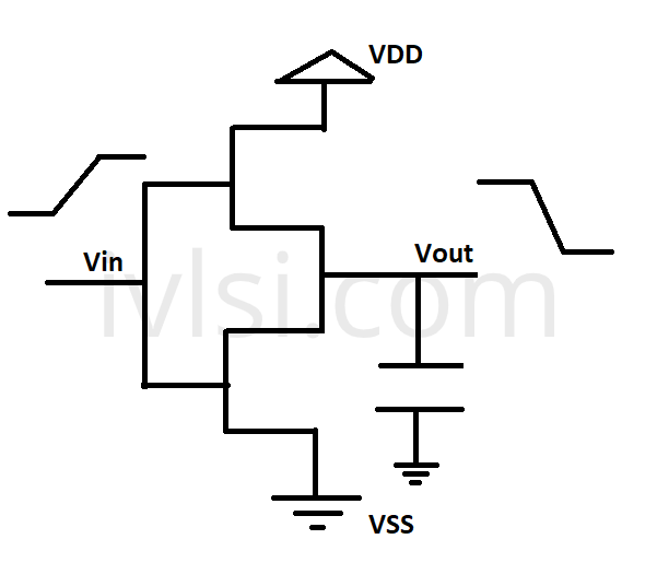
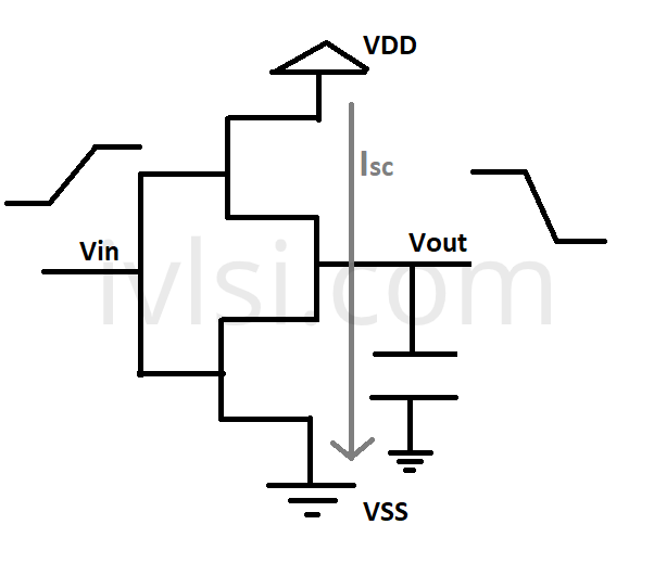
b. Short circuit power (Crowbar current)
There is a situation when PMOS and NMOS transition comes at threshold level. At this time, the PMOS and NMOS are shorted and a rail is getting created from VDD to VSS. The sort circuit between VDD and VSS results into power loss which is called as Short Circuit Power. Since power is getting calculated from current and voltage supply, so the expression comes as per below:
Short Circuit power = VDD * Isc
2. Static Power Dissipation
Leakage power dissipation is named as static power dissipation. Leakage power is getting defined in the library. We have already seen this in Physical Design Inputs section. Theoretically the leakage power dissipation depends on the channel length of the cells. If channel length of the cell is high, then threshold voltage will be high, and leakage will be low. Similarly, we can analyze for the lower channel cells. In one line we can say that lower the channel length cell is more leaky and higher the channel length cell is less leaky.
After placement we need to calculate the leakage power dissipation. Looking at VT profile and leakage numbers we can go for placement exit of the design. Cells can be of type ULVT, LVT and SVT.
- Here ULVT which is ultra-low VT is having maximum leakage but from timing point of view, it is the best.
- LVT is low VT but still it consumes high leakage power and timing is good w.r.t this type of cell.
- SVT is standard VT and timing is not better as compared to ULVT and LVT.
So, in our design we must balance the cells distribution w.r.t ULVT, LVT and SVT. Generally, we avoid using ULVT and we take care to make its use below 15%.