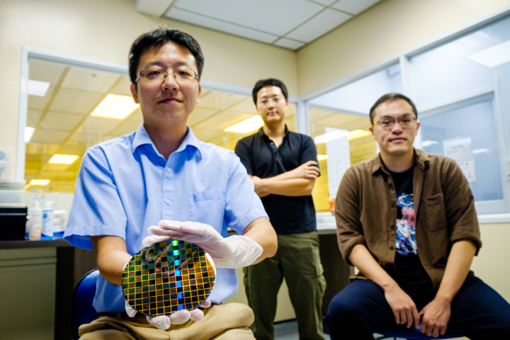
Scientists from Nanyang Technological University, Singapore (NTU Singapore) and the Korea Institute of Machinery and Materials (KIMM) have developed a technique for fabricating highly uniform and scalable semiconductor wafers, paving the way for improved chip yields and low-cost semiconductors.
Semiconductor chips commonly found in smartphones and computers are difficult and complex to manufacture, requiring state-of-the-art machines and dedicated manufacturing environments. They are usually fabricated on silicon wafers and then cut into small chips for use in devices. However, the process is not perfect and not all chips from the same wafer work or perform as expected. These defective chips are discarded, reducing semiconductor yields while increasing production costs. The ability to fabricate consistent wafers with the desired thickness is the most important factor in ensuring that every chip fabricated on the same wafer will function properly.
Nanotransfer-based printing -- a process that uses a polymer mold to print metal onto a substrate by pressure or "stamping" -- has emerged as a promising technology in recent years due to its simplicity, relative cost-effectiveness, and high throughput .
However, this technology uses a chemical adhesive layer, which can lead to negative effects such as surface defects and performance degradation in large-scale printing, as well as harm to human health. For these reasons, mass adoption of the technology and consistent use of chips in devices has been limited.
In their study, published in the peer-reviewed journal ACS Nano, the NTU and KIMM research teams report that their chemical-free printing technique is combined with metal-assisted chemical etching - a method to enhance surface contrast - to visualize nanostructures - resulting in semiconductor wafers with very uniform and scalable nanowires (cylindrical nanostructures). The semiconductor also exhibits better performance compared to current chips on the market. In addition, the manufacturing process is also fast and the chip yield is high. The study is an example of ground-breaking research supporting NTU's 2025 Strategic Plan to address the grand challenges facing humanity and accelerate the translation of research findings into innovations that mitigate environmental and human health impacts.
New Chemical-Free Printing Technology Brings High Chip Yields
A newly developed nanotransfer printing technique developed by NTU and KIMM is to produce highly uniform wafers with Form nanowires by low temperature (160°C) transfer of gold (Au) nanostructure layers onto silicon (Si) substrates during fabrication Can be controlled to the desired thickness.
Chemical-free printing technology works by triggering direct chemisorption of thin metal films under heat—a chemical reaction that creates strong bonds between the substrate surface and the adsorbed species. This industry-standard technology enables the rapid and consistent manufacture of wafers at scale (from nanometers to inches). At the same time, wafers are produced with few defects, meaning few to no chips are discarded due to poor performance.
In laboratory tests, the joint research team was able to achieve over 99 percent yield transfer from a 20-nanometer-thick gold film to a 6-inch silicon wafer. This printable wafer size is limited to laboratory settings, and the NTU-KIMM team believes their technology can easily be scaled up for use on 12-inch wafers - the mainstream wafers in current production lines at semiconductor chipmakers such as Samsung Dimensions, Intel and Global Foundries.
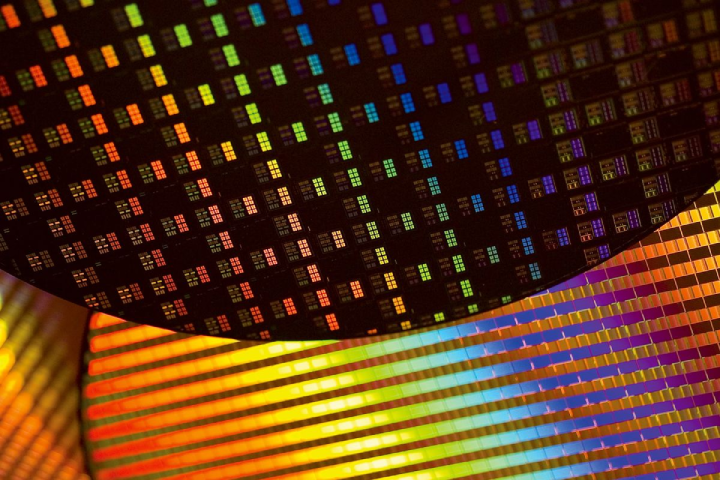
When the process was used to produce 6-inch wafers, the results showed that the printed layers remained intact with minimal bowing during the etching process - a process that often results in layer separation - which provides excellent results for the technology developed by NTU and KIMM. Uniformity and stability are demonstrated. Additionally, when 100 light sensors, called photodetectors, were built into a 6-inch wafer, excellent performance uniformity was achieved, underscoring the technology's huge potential for commercial mass production.
The technology opens the door to cheaper semiconductor chips
Co-principal investigator Kim Munho, assistant professor in Nanyang Technological University's School of Electrical and Electronic Engineering, said the uniformity, scalability and stability of the team's technique overcome major bottlenecks of existing nanotransfer printing methods.
Kim added that the achievements of the NTU and KIMM research teams in developing a cheaper manufacturing process for semiconductor chips could lead to major advances in electronics and light-based devices. "The technology developed by the research teams at NTU and KIMM has been shown to be effective in producing wafers with excellent uniformity, thereby reducing defective semiconductor chips. The reality of global chip supply is that it is susceptible to many external factors, Includes material shortages and unexpected events, such as supply chain disruptions caused by the COVID-19 pandemic. Therefore, our newly developed process has the potential to ease future global chip supply by improving chip yield. In addition, chipmakers can enjoy greater cost efficiencies and higher yields," Kim said.
Emphasizing the importance of this work, co-lead author Dr. Jeong Jun-Ho, Senior Research Fellow in the Nano-Fusion Manufacturing Systems Research Department at KIMM, said, "The technology developed by the NTU-KIMM team is a new advancement in low-cost, large-scale production technology. Concept for highly unified and scalable. "Semiconductor nanostructures that can be applied to mass production of nanophotonics, high-performance nanosolar cells, next-generation secondary batteries, and more."