In the month of May, U.S. President Joe Biden toured the Samsung campus in Pyeongtaek and toured a state-of-the-art factory that will use the 3-nanometer process node. Industry insiders expect the South Korean giant to announce the start of mass production in the coming days and beat rival TSMC in its quest for the world's most advanced chips.
Samsung is ambitious for its semiconductor division and is a key part of its $205 billion plan to conquer chipmaking, robotics, artificial intelligence and biopharmaceuticals. No less than half of these funds go to advanced chip factories and research and development of new process nodes and new transistors.
However, the South Korean tech giant has encountered a number of revenue issues as it moves to smaller process nodes, which has affected some of its biggest customers, such as Qualcomm, which is now considering TSMC for future mobile chips. After addressing yield issues and relatively low power efficiency with Ampere GPUs based on Samsung's 8nm process node, Nvidia is turning to TSMC's next generation.

With a revitalized Intel led by Pat Gelsinger, competition in semiconductor manufacturing is heating up. Samsung needs to beat the rest in the 3nm commercial manufacturing race, or it won't be able to attract big customers like Nvidia, AMD, Apple, etc. TSMC says it will start ramping up mass production of the 3nm process in the coming months, so the window is smaller.
Samsung knows this and works hard to meet TSMC's schedule. But while the company plans to start producing 3nm chips by the end of the month, that timeline may be a little too optimistic. In April, Samsung Foundry executives told investors that commercial production would begin in a few weeks, but we haven't had an official update on the matter. Reports in local South Korean media suggest that Samsung is preparing to announce the start of 3nm mass production, possibly as early as this week. It will be a major showcase for rival TSMC, and it will also mean the South Korean company will be the first to use gate-all-around field-effect transistors (GAAFETs).
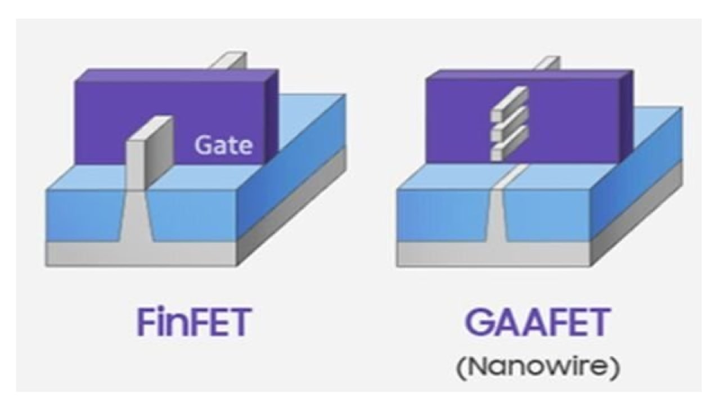
Samsung calls its implementation of a 3nm GAAFET transistor a multi-bridge channel field effect transistor, but that's just the technical name for a transistor that consumes 50% less current, takes up 45% less space, and can operate at very low voltages more stable operation. Samsung is also rumored to be attracting initial customers for the new process node, so it will be interesting to see if the company can avoid repeating its 8nm and 4nm failures. Either way, the foundry business is a big contributor to Samsung's bottom line, as more than half of its operating profit -- about $6.7 billion and change is coming from the chipset division.