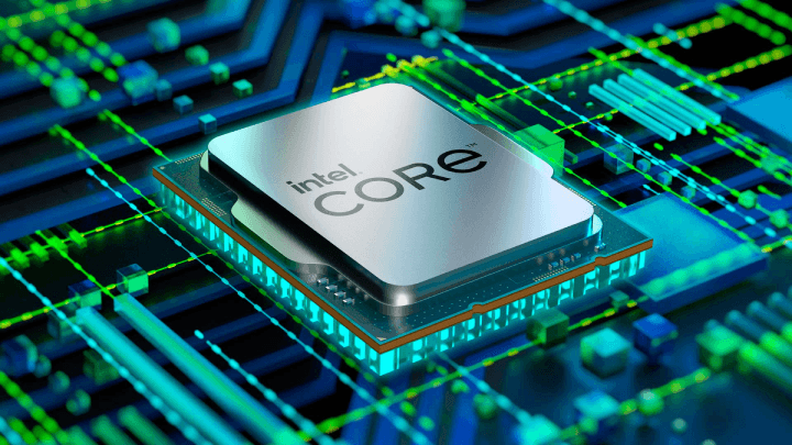
You might not be aware that Intel makes photonic modules for data center optical computing links, but the company has been in the business for years. Intel Labs has been researching ways to reduce the cost of these modules using automated semiconductor manufacturing techniques since the early 2000s.
In the year 2006, Intel and the University of California, Santa Barbara (UCSB) announced the construction of the world's first electric hybrid silicon laser using standard silicon fabrication processes. This laser fuses the light-emitting properties of indium phosphide (InP) with the optical conductivity of silicon, forming a single hybrid semiconductor laser chip by fusing strips of InP onto a silicon wafer. Now, Intel Labs is building on this work by announcing the successful construction of an eight-wavelength distributed feedback (DFB) laser array on a chip that delivers excellent output power and wavelength spacing uniformity that exceeds industry specifications for optical laser communication modules. This semiconductor element is the basic element of wavelength division multiplexing (WDM) lasers used for high-speed optical communications in data centers.
A WDM laser array produces multiple beams of different frequencies that can be combined on a single fiber, pushing a larger bandwidth through the fiber than would be possible with a single-frequency laser. In Intel's recent announcement, an experimental eight-laser DFB array produces eight beams of infrared light with a channel spacing of 200 GHz. Like the hybrid silicon laser announced in 2006, the DFB laser array combines the light-emitting properties of indium phosphide (InP) with the light-manipulating capabilities of silicon, but in a much more complex way.

First, a grating etched in silicon sits next to each InP light emitter and modulates the light from each emitter. The physical division of each of the eight gratings allows each laser to produce a precise beam at a different frequency. The gratings were fabricated on Intel's standard 300mm CMOS wafer production line using deep ultraviolet immersion lithography, a high-volume, low-cost process. Light guides, modulators, combiners and detectors are also etched into silicon using the same high-volume CMOS process technology. V-grooves cut into silicon using anisotropic etching are used to precisely align the optical fibers on the photonic hybrid chip. All key components of high-speed optical transceivers are fabricated simultaneously on optical integrated circuits.
The ability to manufacture the most critical photonic components as hybrid monolithic chips will allow Intel to significantly increase the bandwidth of its optical modules while reducing their cost compared to today's modules. Rong Haisheng, senior principal engineer at Intel Labs, said the technology can be extended beyond eight-laser arrays to create photonic components that simultaneously generate, modulate and combine 16 or 32 wavelengths, opening up broad applications for the technology scope.
In addition to developing new, faster optical communication modules for data centers, these semiconductor lasers are particularly well suited for Intel's chiplet manufacturing method, in which various semiconductor chips are packaged together to form a more complex device. In the long run, chiplet manufacturing is a way to extend the life of Moore's Law.
Development of single-chip DFB laser arrays as chiplets enables co-packaged optics. That means Intel can design CPUs, GPUs, FPGAs, memory modules and storage devices that all communicate optically rather than using copper cables. With current communication rates exceeding 100 Gbit/s, and optical communication being more energy-efficient than electrical communication, the technology is expected to revolutionize chip-to-chip connectivity.